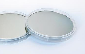
Ge wafer
Germanium, as a rare metal, has many special properties: good chemical stability, strong corrosion resistance, easy processing, high and uniform transmittance and high refractive index, high radiation resistance, high frequency, good photoelectric performance.
In the semiconductor industry, aerospace industry, high frequency and high frequency electronics, optical fiber communication, electronic devices, PET catalysts, infrared optics, solar cells, chemical catalysts, biomedical and other fields have a wide range of important applications.
2-6 inch germanium sheet, thickness 150um+, conductive type: N type, P type, non-doped.
Typical specifications are shown in the following table:
Semi-conducting Ge Specifications
| Growth Method | VGF |
| Dopant | n-type: As; p-type: Ga |
| Wafer Shape | Round (DIA: 2" 4" 6") |
| Surface Orientation | (100)±0.5° |
Other Orientations maybe available upon request
| Dopant | As (n-type) | Ga (p-type) |
| Resistivity (Ω.cm) | 0.05-0.25 | 0.005-0.04 |
| Etch Pitch Density (cm2) | ≤ 300 | ≤ 300 |
| Wafer Diameter (mm) | 50.8±0.3 | 100±0.3 |
| Thickness (µm) | 175±25 | 175±25 |
| TTV [P/P] (µm) | ≤ 15 | |
| WARP (µm) | ≤ 25 | ≤ 25 |
| IF* (mm) | 17±1 | 32.5±1 |
| OF (mm) | 7±1 | 18±1 |
| Polish | E/E, P/E, P/G | E/E, P/E, P/G |
| Backside Ra (µm) | < 0.1 | < 0.1 |